|
Async1 Chip:
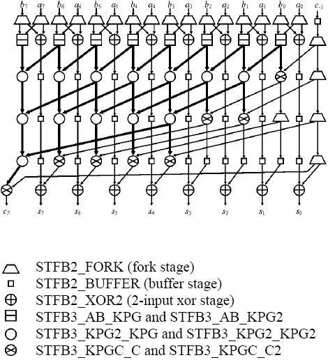
Asynchronous 1.45 GHz Prefix Tree Adder
|
| |
|
| General Description:
The USC Async1 chip has been successfully fabricated
and tested in 2004. A 64-bit asynchronous prefix adder has been
fabricated to show the performance and specifications of
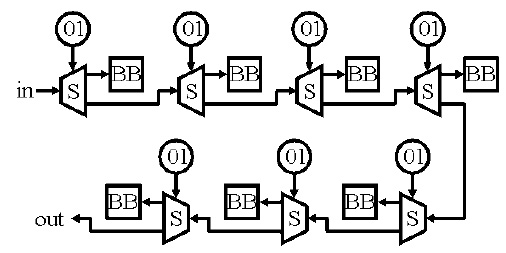
STFB
standard cell design which provides low latency and fast cycle time
at the expense of some timing assumptions. The high level design of
the chip has been entered through a schematic of our library cells (Virtuiso).
Silicon Ensemble has been used for place and route. The chip is
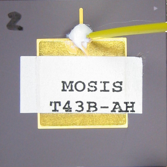
fabricated using MOSIS TSMC 0.25 um technology.
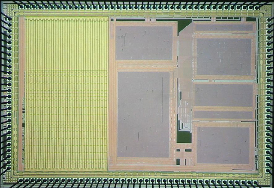
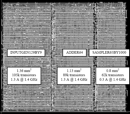
The chip consists of three parts:
The input generator:
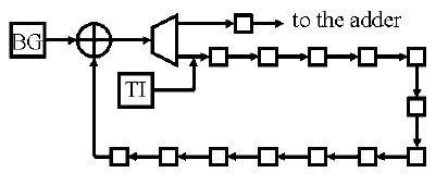
This block generates a test pattern to be fed to
the adder. The TI block insert a token in the pipeline, and the BG
is a controlled bit generator.
The adder
Click on the right image for a bigger picture
The output sampler:
In order to test the adder running at full
throughput, an output circuitry has been implemented that samples
the result (which is 65 bits, including carry). This unit forwards
the result to the output each 128 times that a result has been
generated so that a much slower circuit can read and compare the
results of the iteration #1, #129, #257, ... |
 |
 |
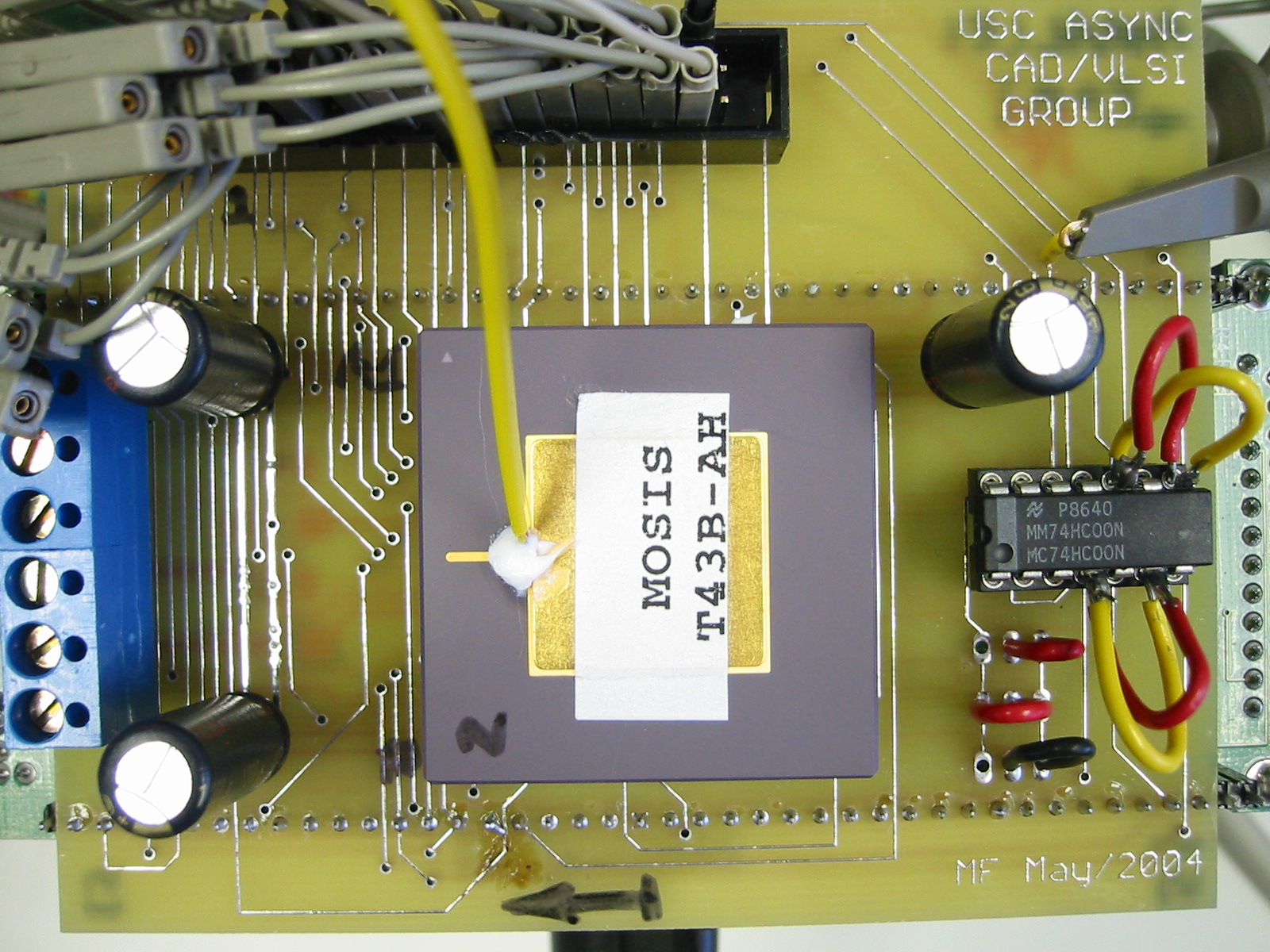
| Test Board:
To test the chip, an interface board has been designed
which connects to an FPGA evalution board. The FPGA is a
XILINX
XCS2100 Spartan II on a
Xcess XSA prototyping board. The
software utilized to program the FPGA was ISE V.6, and the Xcess too
package. Once programmed, the FPGA loads the STFB input block with
the operands, sets the sample rate in the output block, and runs the
chip by acknowledging all requests as the come out of the chip.
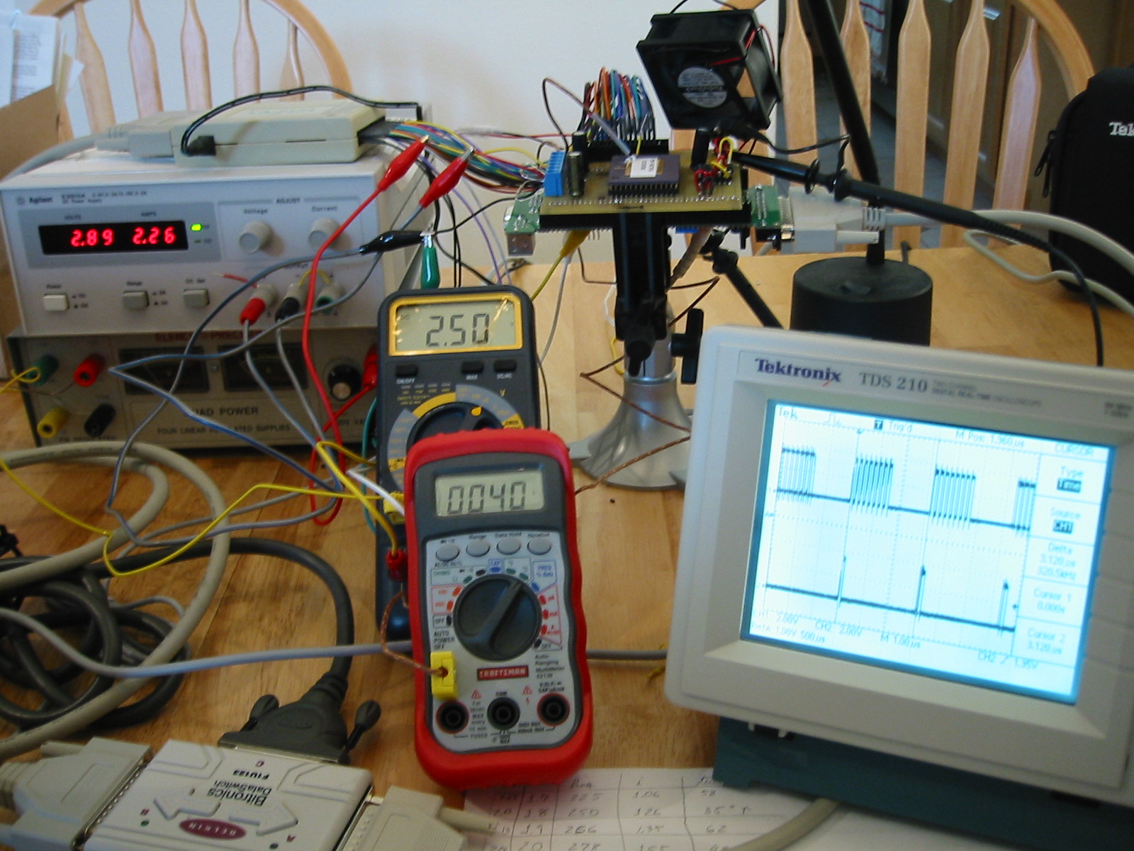
An oscilloscope (Tektronix TD2 10) is used to
check the byte and carry acknowledge signals. One multimeter is used to
measure the temperature on top of the package while another displays
the on-chip voltage. The current is measured by the power supply (Agilent
ES 61 OA). A 24-charniel logic analyzer (Link Instruments LA-2 124)
is used to capture the waveforms, which allows checking the
initialization and operation of the demonstration chip. For some
clips of the chip performance, go to the bottom
of this page.
|
|
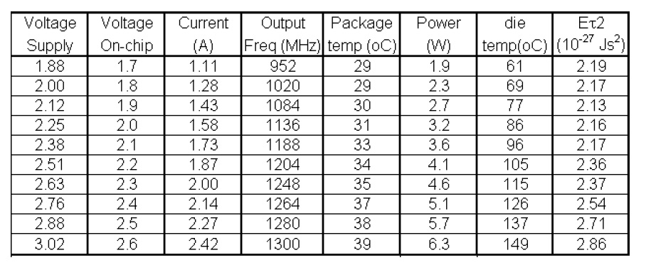
| Results:
Our first fabricated chip works without any error,
and generates the expected results at 1.45 Ghz (with cooling fan).
The following table shows the results of our tests:
|
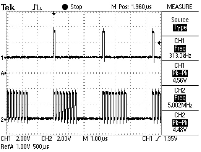
(Oscilloscope View)

(Logic Analyzer View, at 1.25Ghz) |
|
Clips:
Here are some demo clips of the chip performance. The difference
between sampling and non-sampling mode is described
here, and the description of
the results is here.
|
| Publications:
For more information please visit
the following links:
- Thesis:
Single-Track Asynchronous Pipeline Template, M. Ferretti, Ph.D.
Thesis, University of Southern California, Jun, 2004.
- Paper:
High Performance Asynchronous ASIC Back-End Design Flow Using
Single-Track Full-Buffer Standard Cells, M. Ferretti, R.O. Ozdag and
P.A. Beerel, 10th Symposium on Asynchronous Circuits ASYNC,
Herssonissos, Crete, Greece, April 2004.
|
|
|
|
Home | Publications
| People |
Research
USC |
Viterbi School of Engineering | EE
Department |
|
The USC Asynchronous CAD/VLSI Group
Hughes Aircraft Electrical
Engineering Center EEB 100 Los Angeles, CA 90089-2560 |
|