|
USC Async1 Chip - 1.45 GHz 64-bit Asynchronous Adder |
|
 |
1
General Description
The
USC Async1 chip was fabricated in March 2004 using TSMC 0.25
um
process. It comprises two test circuits:
�
A 64-bit asynchronous prefix adder with input
generator and output sampler blocks. All blocks were
fabricated to show the high performance of the proposed
STFB (Single-Track Full-Buffer) standard cell design,
which provides low latency and fast cycle time.
�
A Sequential Decoder implemented with QDI
(Quasi-Delay Insensitive) standard cells (this circuit is
under test).
2
STFB template
In
the STFB cell template, shown below, the Right Completion
Detection circuit (RCD) allows the cell to work only
if the output channel (R) is empty, and the State
Completion Detector circuit (SCD) removes the input
data from the input channel (L) when it is no longer
needed.
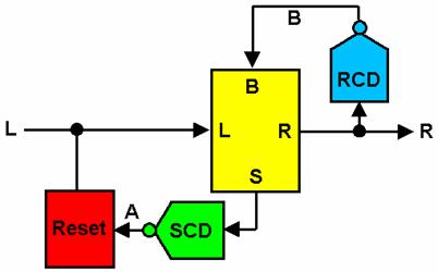
Basic
internal diagram of a STFB cell. |
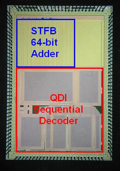
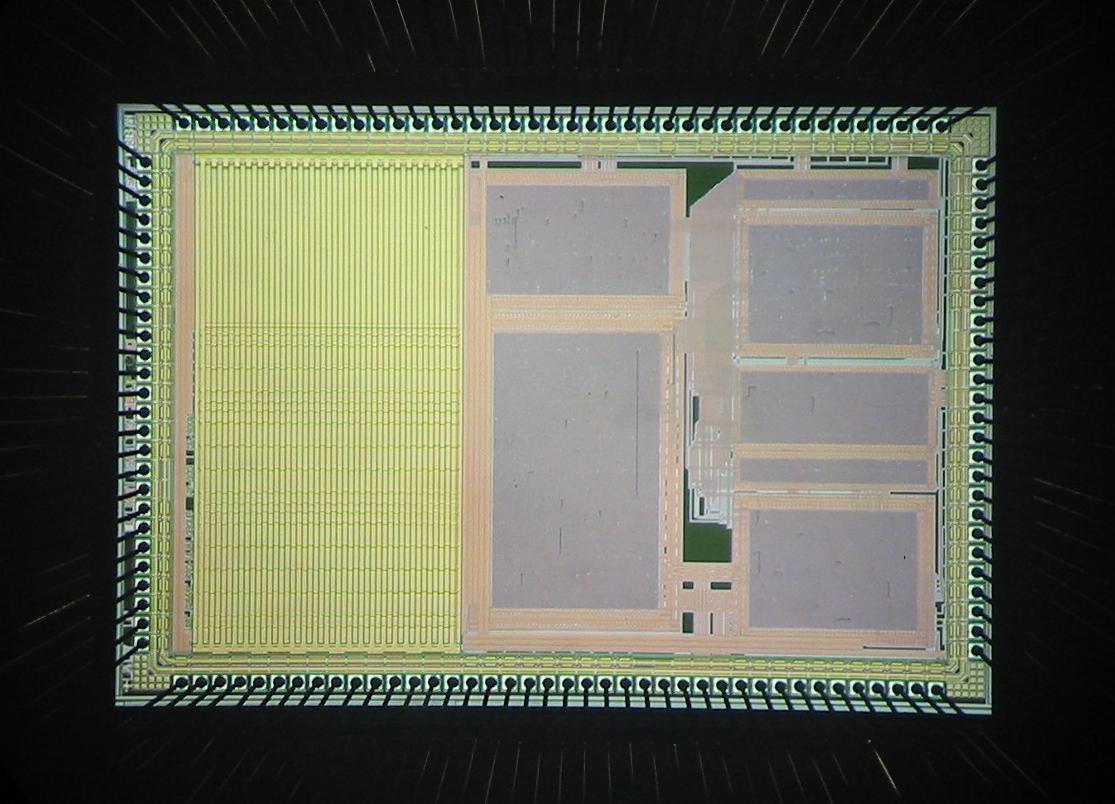
Async1
die photo (bigger
picture). |
|
3
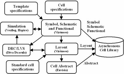
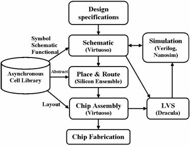
STFB standard cell library
The
STFB cells were created using Cadence Custom IC Design and
Synopsys tools (see
publications below), and were made freely available
through
MOSIS Educational Program. The figure below illustrates
the library creation process.
 |
4
STFB block design
Using
the STFB library, the circuit blocks described below were
designed as follows:
 |
|
5
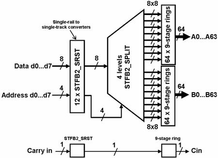
INPUTGEN block
With the
STFB library, the input pattern generator for the adder was
designed as shown in the block diagram below. The INPUTGEN
circuit allows 64-bit operands and 1-bit carries to be
loaded to 9-stage rings that will continuously feed the
adder inputs.
 |
6
The
9-stage ring
The
INPUTGEN block has 129 rings with 9-stages each (9 STFB
cells in a loop) as show in the block diagram below. These
rings can load up to 7 different bits that will be
continuously duplicated and send to the adder inputs. All
the 129 rings allow us to load the up to 7 sets of numbers
we want to add (each set with 64-bit for each A operand,
64-bit for each B operand and 1-bit for each carry in).
 |
|
7
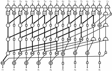
ADDER64 block
The
figure below represents an 8-bit prefix adder implemented
with STFB cells. The thin arrows are dual-rail channels (2
wires), while the thick arrows are 1-of-3 channels (3
wires). The 64-bit version implemented in our design is an
extension of the diagram below.
 |
8
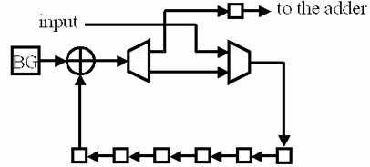
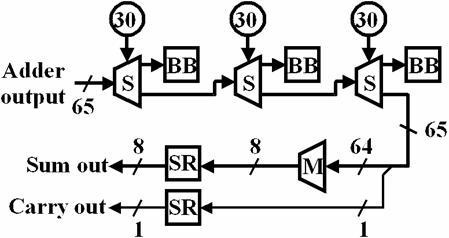
SAMPLER block
Due to the high-performance of the
STFB cells, it is necessary to sample the output results in
order to avoid slow down the adder. The circuit shown in the
diagram below allows us to select the sample rate and also
multiplex the result in order to output one byte at a time.
 |
|
9
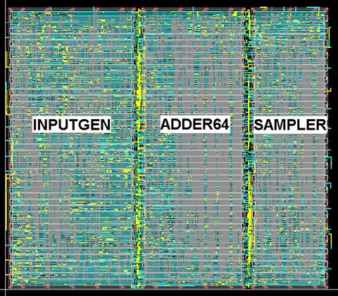
Circuit layout
The
layout of the three blocks were automatically generated and
placed side-by-side as shown below. The three blocks have
260k transistors in 3.3 mm2. The power grid (not
shown) on top of the blocks was designed to supply the high
current required when running at full throughput (28 pads
were allocated for power supply).
 |
10
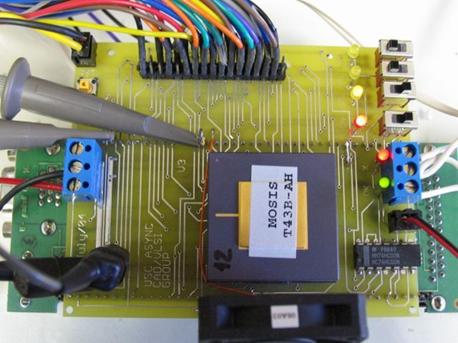
Test board
To
test the chip, an interface board, shown below, has been
designed which connects to an FPGA evaluation board. The
FPGA is a
XILINX XCS2100 Spartan II on a
Xess XSA prototyping board. The software utilized to
program the FPGA was ISE V.6 and the Xess package. Once
programmed, the FPGA loads the STFB INPUTGEN block with the
operands, sets the sample rate in the SAMPLER block, and run
the chip by acknowledging all requests as they come out of
the chip.
 |
|
11
Test setup
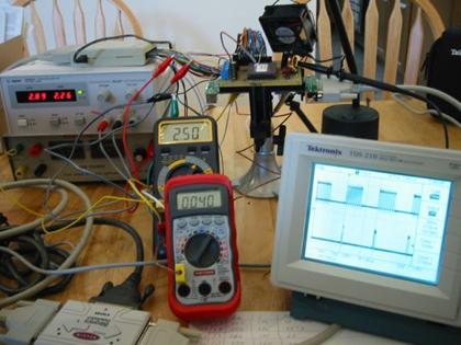
An
oscilloscope (Tektronix TDS210) was used to check the byte
and carry acknowledge signals. One multimeter was used to
measure the temperature on top of the package (40oC!!),
while another displays the on-chip voltage (2.5V). The
current (2.26A) was measured by the power supply (Agilent
ES610A). A 24-charniel logic analyzer (Link Instruments
LA-2124) was used to capture the waveforms, which allows
checking the initialization and operation of the
demonstration chip. For some clips of the chip performance,
go to the bottom of this page.
 |
12
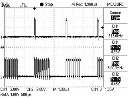
Performance
The
figure below is the acknowledgment signals for the carry and
for the eight bytes outputted by the SAMPLER block. In this
example, since acknowledge frequency was 313kHz and the
sample rate was set to 1:3971, the internal adder throughput
was 1.24GHz. This is an impressive performance
when considering the technology (0.25 um)
and the fact that the layout was automatically generated
using a conventional back-end flow, which resulted in a
simple, fast and efficient design process that can be easily
understood by synchronous designers.
 |
|
13
Test results
The
STFB circuits, fabricated in the Async1 chip, worked
perfectly, and generated the expected results (very
close to the Nanosim simulations) reaching up to at 1.45
GHz (with cooling). The following table shows the
results of our tests at room temperature with a fan over the
chip under test.
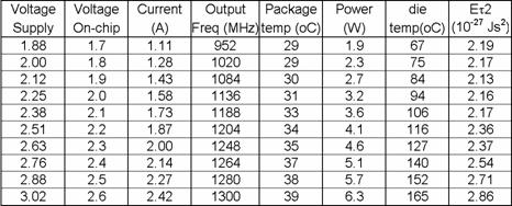
STFB
circuits at full speed at room temperature with fan.
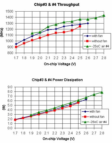
The
graphics on the right show the throughput and power
dissipation of sample #3 and #4 running at full speed. Chip
#3 was tested at room temperature with and without fan. Chip
#4 was tested with air at -25oC blowing on top of
the device. Notice that, since the STFB circuits are
asynchronous, the performance automatically adjusts
according to the supply voltage and temperature. Also,
notice that, with cooling, the STFB circuits reached the
impressive mark of 1.45 GHz. |
 |
|
14
Conclusion
STFB
templates
were
proposed for high-speed area-efficient asynchronous
non-linear pipeline design. A freely available STFB standard
cell library using TSMC 0.25
um
technology was generated and posted with MOSIS Educational
Program. A complete STFB design with 260k transistors
was successfully implemented and tested reaching 1.45 GHz.
The templates have higher throughput
than the fastest known QDI templates and have less timing
assumptions and lower latency than the most aggressive GasP
templates. Consequently, for systems that are
latency-critical, STFB templates may yield a significant
performance advantage. It also offers a small cycle time
that allows the STFB circuits to operate at very high
throughputs with small distances between consecutive data
tokens, resulting in smaller and faster circuits than their
QDI alternatives.
|
15
Publications
For
more information please visit the following links:
-
Thesis:
Single-Track Asynchronous Pipeline Template, Marcos
Ferretti, Ph.D. Thesis, University of Southern California,
Jun, 2004.
-
Papers:
-
Single-Track Asynchronous Pipeline Templates using 1-OF-N
Encoding, M. Ferretti and P. A. Beerel, DATE'02,
Paris, France, March 2002.
- High Performance Asynchronous Design Using
Single-Track Full-Buffer Standard Cells, M. Ferretti and
P.A. Beerel, IEEE Journal of Solid-State Circuits, Vol.
41, No. 6, pp. 1444-1454, June 2006.
-
High Performance Asynchronous ASIC Back-End Design Flow
Using Single-Track Full-Buffer Standard Cells, M.
Ferretti, R.O. Ozdag and P.A. Beerel, 10th Symposium on
Asynchronous Circuits ASYNC, Herssonissos, Greece, April
2004.
|
|
16
Acknowledgements
This
research has been partially supported by NSF Grant
CCR-0086036 and gifts from TRW, Fulcrum Microsystems and the
MOSIS Educational Program. Thanks to Jay Moon for his
valuable help with the CAD tools, to Sachit Chandra for his
help with the design flow and Sunan Tugsinavisut for many
helpful discussions.
Nanosim
and Hspice are trademarks of Synopsys, Inc. (Mountain View,
CA). Dracula, Verilog, Virtuoso, Envisia and Silicon
Ensemble are trademarks of Cadence Design Systems, Inc. (San
Jose, CA). All other trademarks are proprietary of their
respective owners.
|
|


